Transistors and TTL IC’s
Welcome. This is going to be the transistor-transistor logic (TTL) post. We’ll go over what a transistor is, why they’re useful, and a couple of example circuits. Finally, we’ll take a look at the 74xx series of TTL integrated circuits, the backbone of this project.
Disclaimer: not an expert.
Transistors
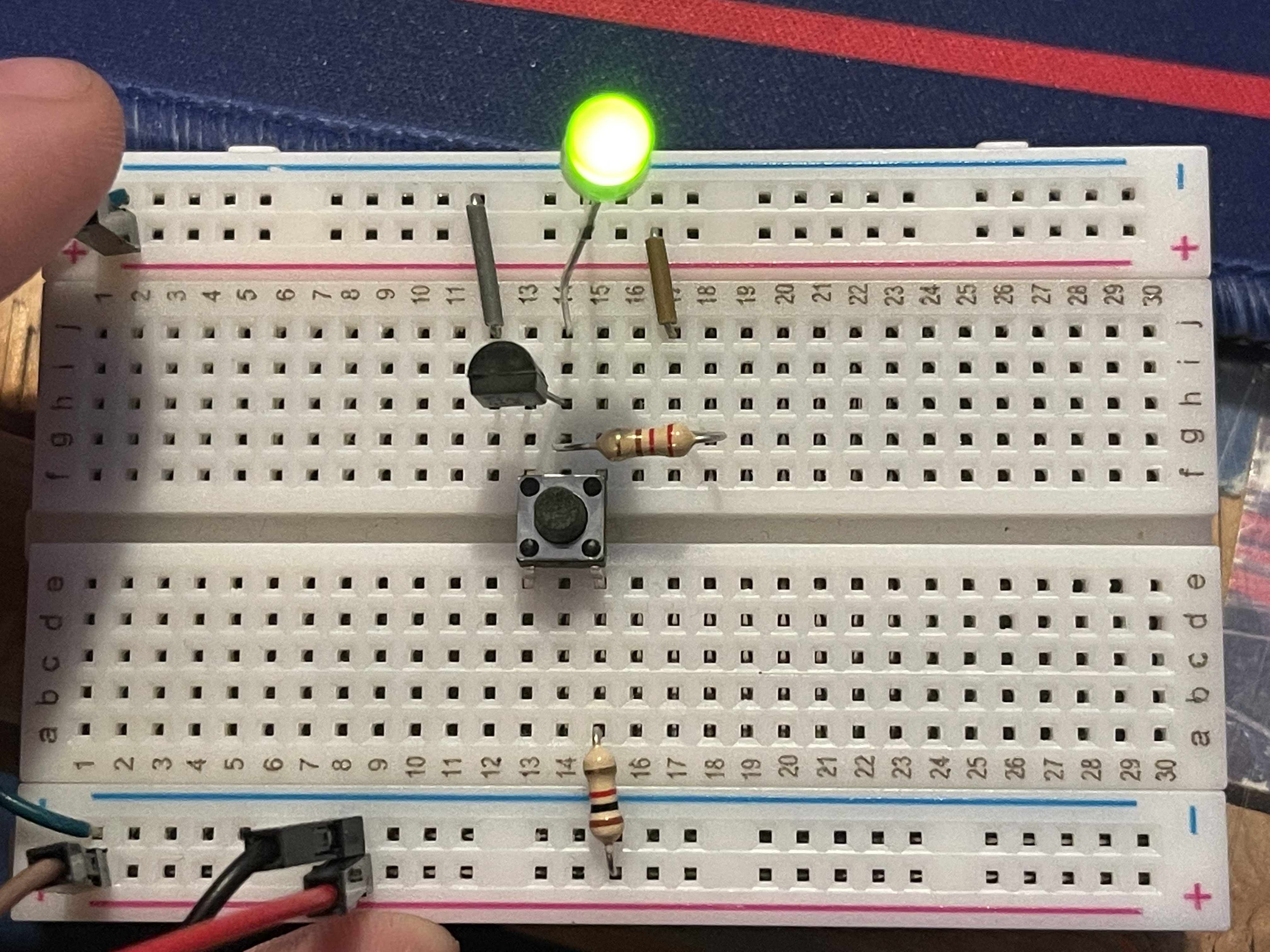
Transistors can come in many forms and have a wide variety of use cases, but we’re only interested in one of those forms (NPN Bipolar Junction Transistors) and primarily in one of their uses - an electrically controlled switch. Consider the following circuit with a pushbutton switch:
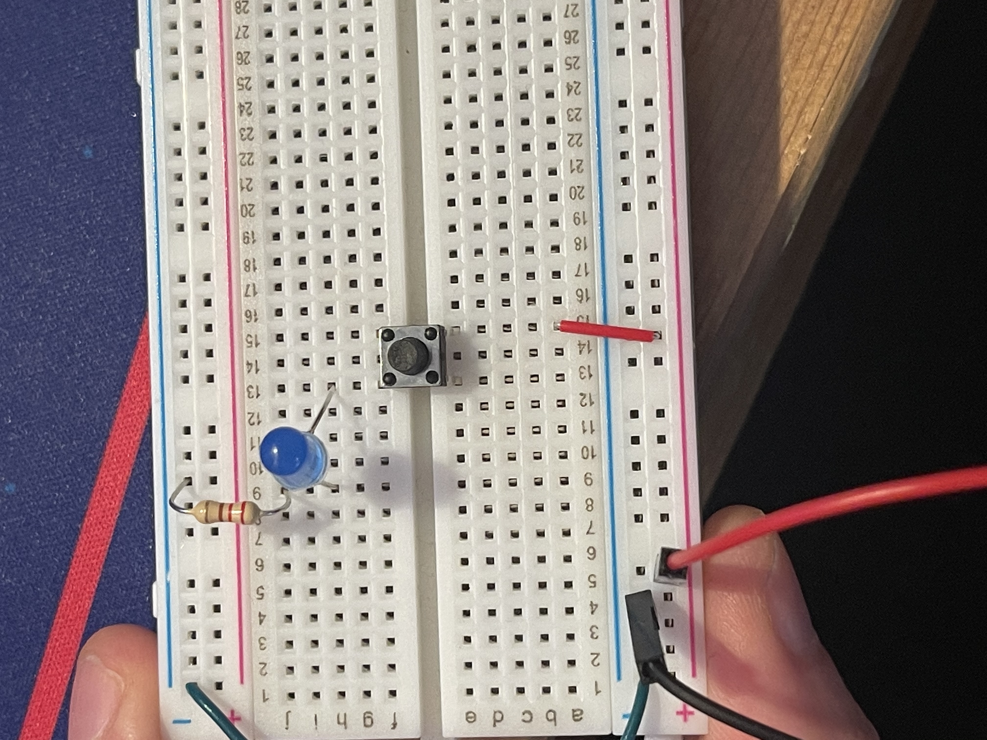
Without the button depressed, there is no connection between the positive and negative power rails. Current can’t flow from the positive power rail, through the switch, through the LED, and to ground. But while the button is pressed, the circuit completes, and current flows from positive to negative, through the LED.
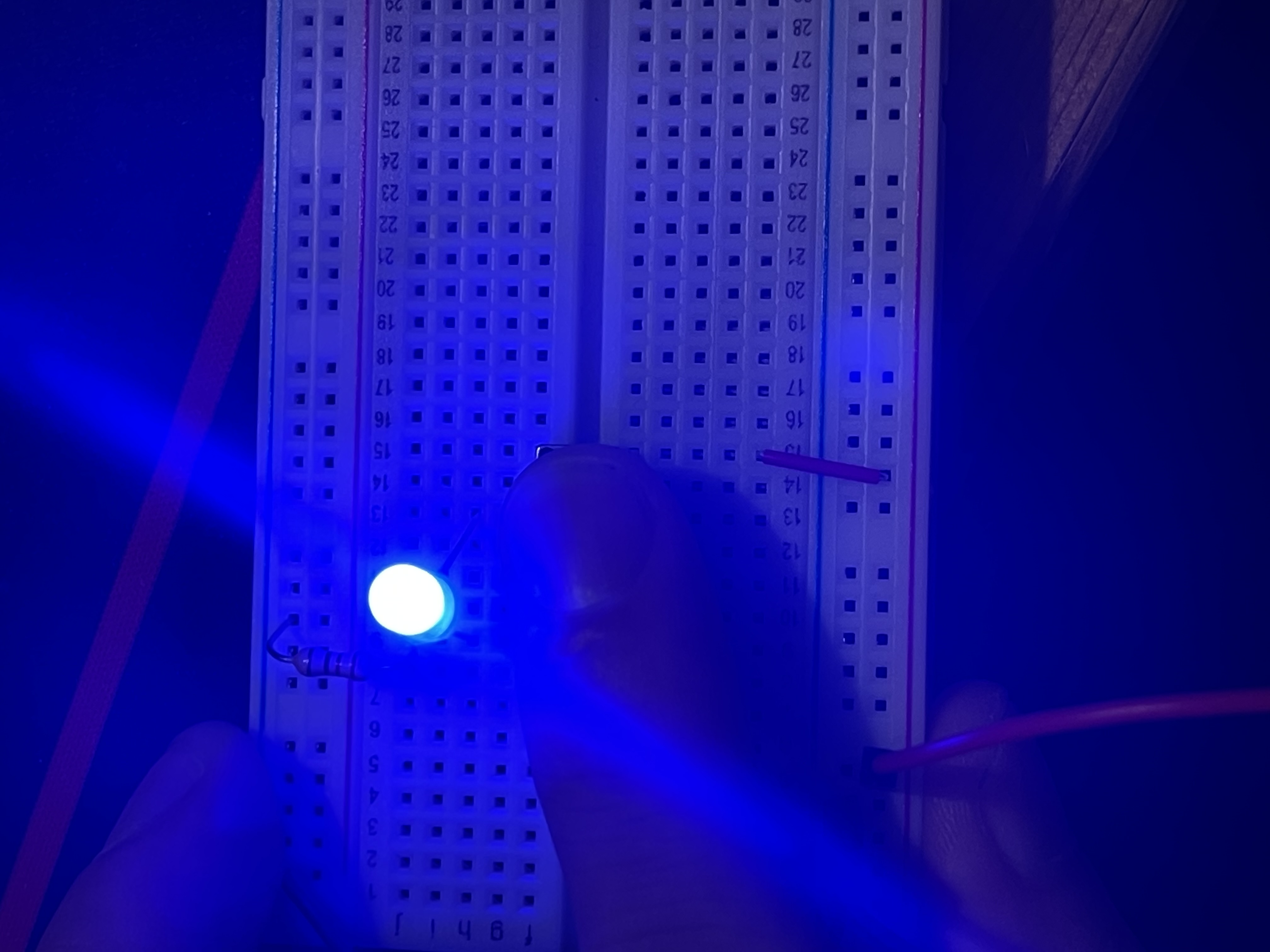
This effectively gives us some rudimentary conditional logic. If the button is pressed, the output value (connected to the LED) is on, otherwise, its off.
Transistors give us something similar, except instead of pressing a button, we make use of a digital signal. Let’s look at the schematic symbol for a transistor.
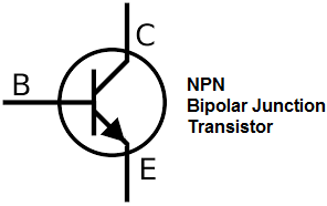
It has 3 terminals: Collector (C), Base (B), and Emitter (E). The base is our input, when we apply a small current between this terminal and the emitter, a larger current begins to flow between the collector and the emitter. In this case, applying a current to the base is like pressing down on the switch: it completes the circuit between the other terminals.
Transistors can be linked together in different ways to make logic gates, which is what we care about for building this processor.
NAND Gates
A NAND gate is an inverted AND gate. The output of an AND gate is only 1 (also called true or HIGH) when all of its inputs are true. If you invert the output (every 0 becomes a 1, every 1 becomes a 0), you get a NAND gate, the output of which is 1 in every case except when both inputs are 1. Truth table below:
| A | B | Out |
|---|---|---|
| 0 | 0 | 1 |
| 1 | 0 | 1 |
| 0 | 1 | 1 |
| 1 | 1 | 0 |
NAND gates are pretty important because they’re what is sometimes called a Universal Gate. This means that any boolean expression (sequence of logic gates) can be expressed using exclusively NAND gates. I won’t cover a proof here, but check out the wikipedia page on NAND logic if you want to see some examples.
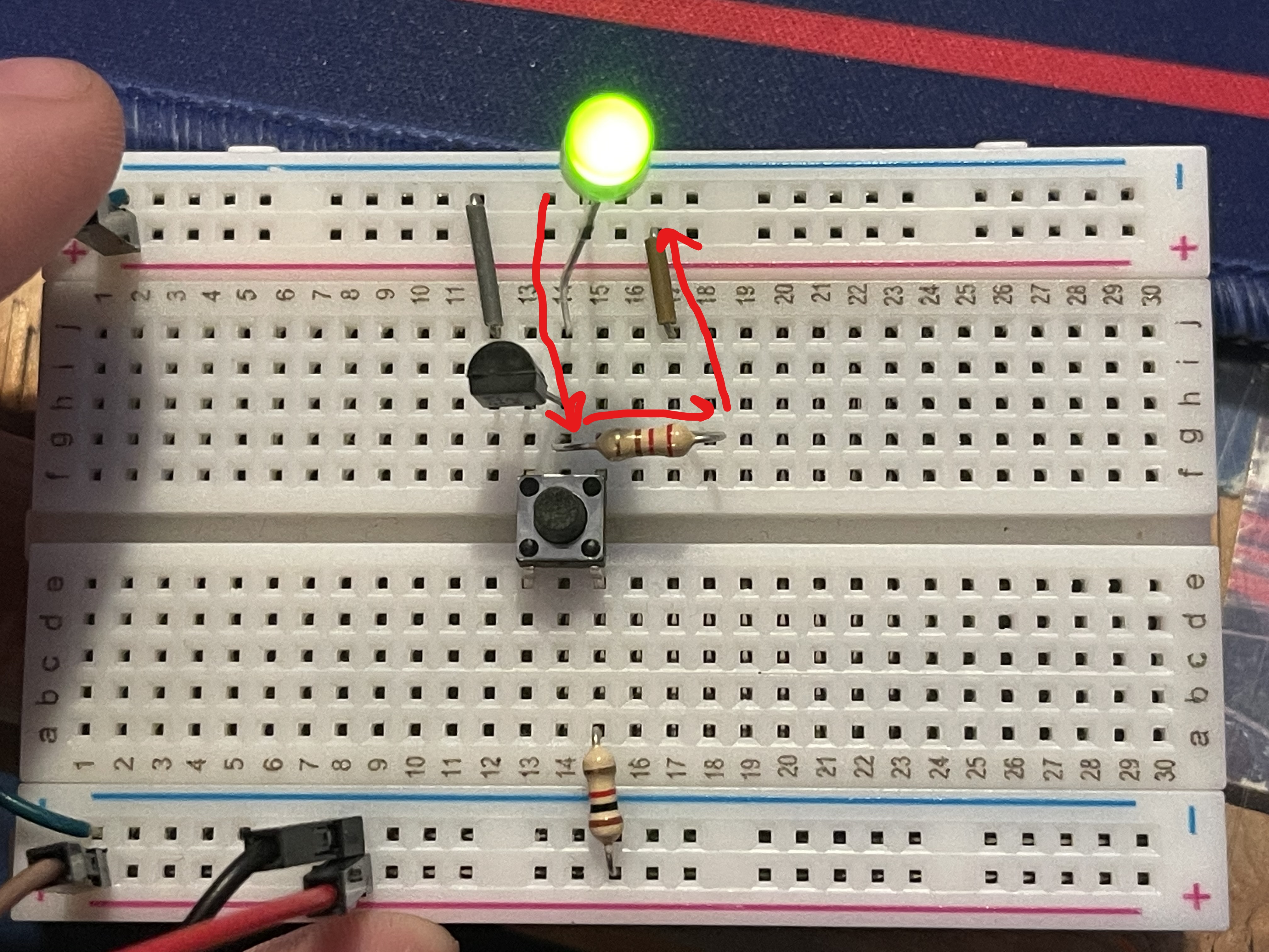
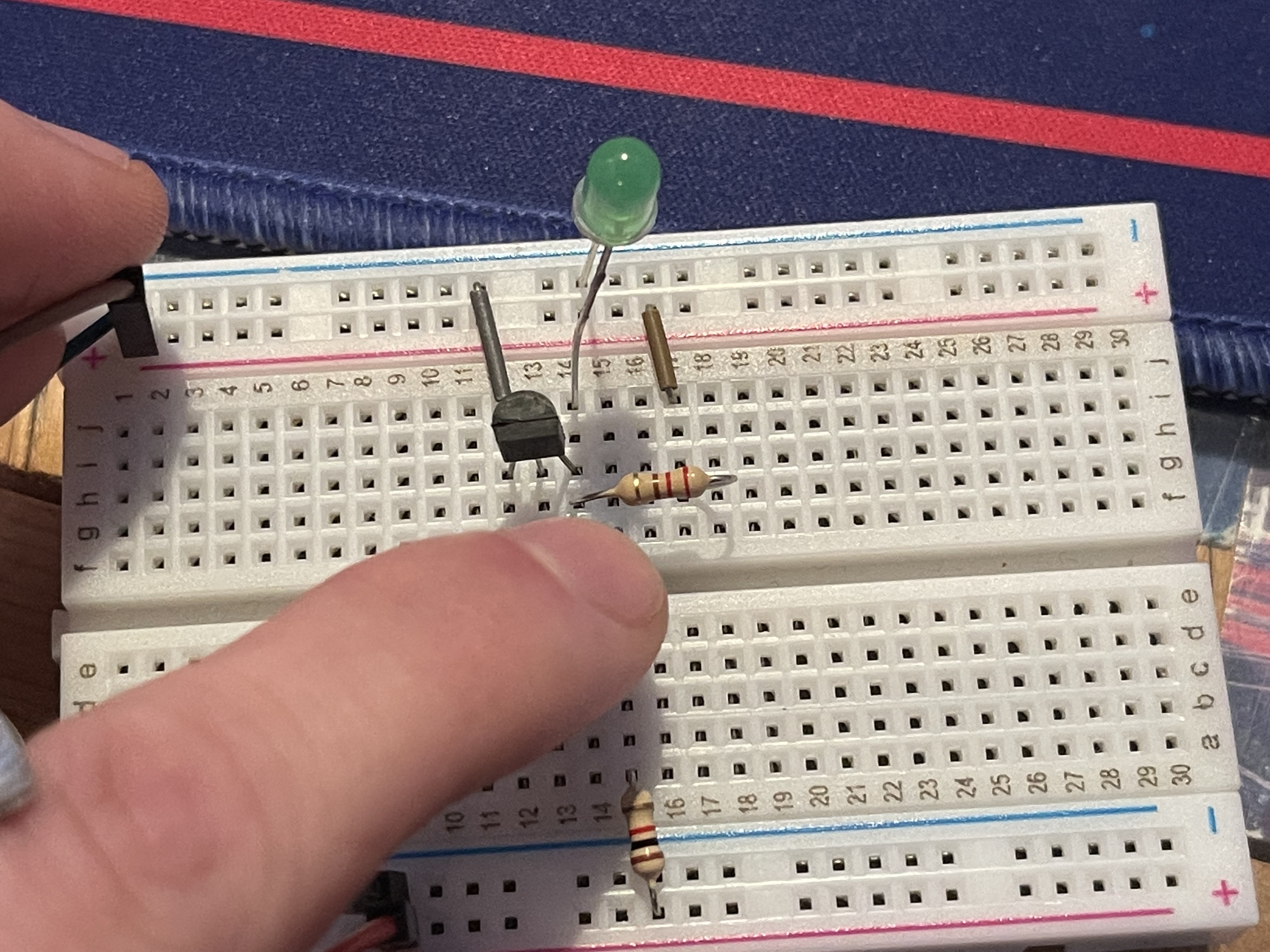
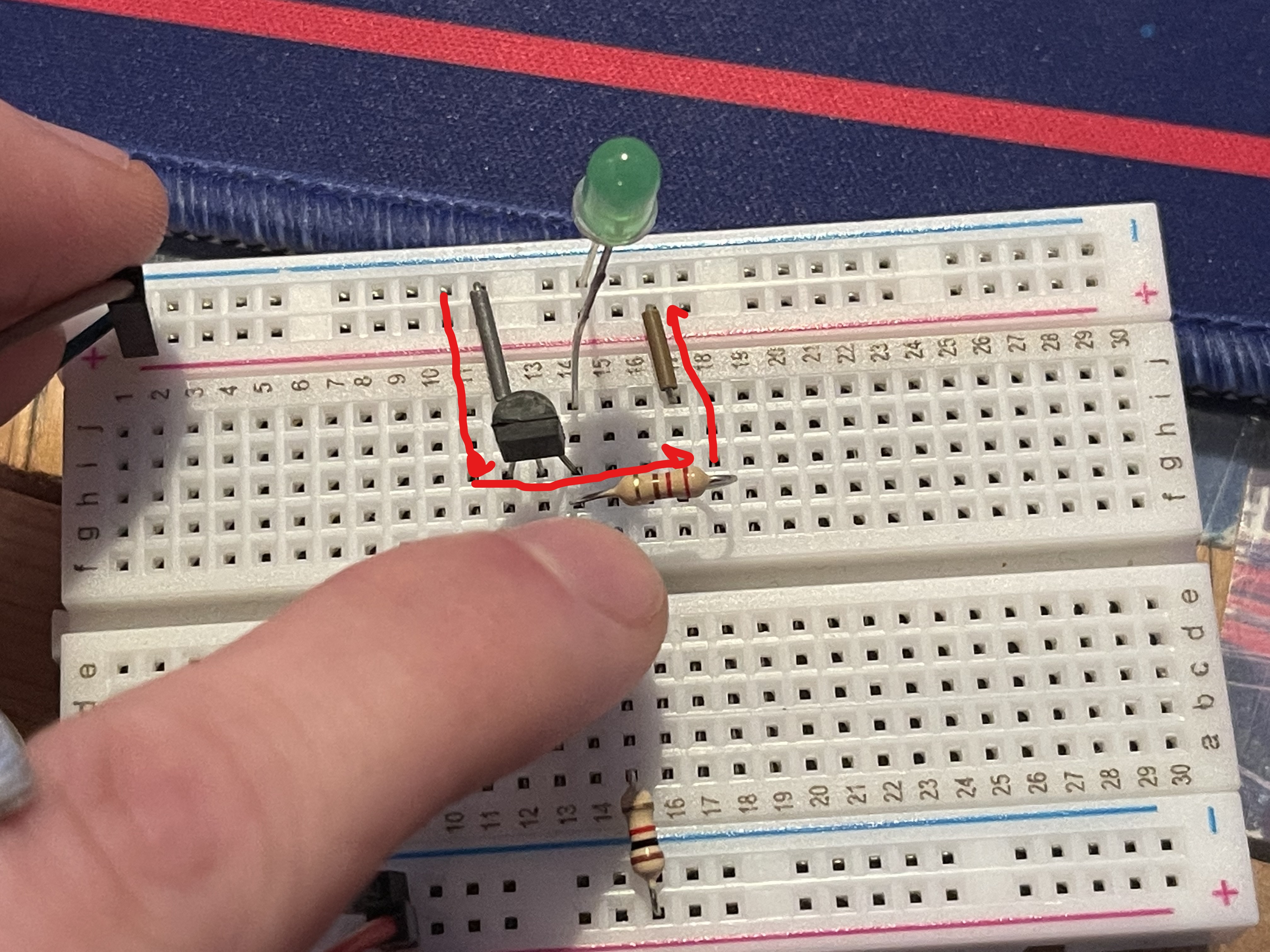
Let’s make one out of transistors. We need two things: an inverter, and an AND gate. Lets start out with the inverter. The leftmost pin is the collector, the middle pin is the base, and the rightmost pin is the emitter. In the top picture, the input to the base is a 0, so the only complete circuit between 5V (positive) and ground (negative) is through the resistor and LED (second picture). When the input to the base is on, then current can flow between the collector and the emitter. Since the collector and the LED are tied to ground, the voltage differential between the LED and the resistor becomes 0. When this happens, current wont flow through the LED, and instead will pass through the resistor to 5V, thus turning the output off.
An AND gate is even more simple to construct. The emitter of the A input transistor is tied to the collector of the B input transistor, the emitter of which is our final output. In order for current to flow between the collector of A and the emitter of B, a current needs to be applied to the base of each. If just the A input is on and B is off, then the circuit remains incomplete as current can’t flow from the collector to the emitter of B. Likewise, if only B is on, then current can flow from it’s base to emitter, but no current is reaching the collector, as this requires A to be on.
If we connect the emitter of B to the base of the inverter circuit above, then we have a NAND gate, and could theoretically build any logic we want. If we wanted to build this processor entirely out of discrete transistors like this, we certainly could, but I’m more interested in the computer architecture aspect, so instead we’ll make use of integrated circuits that give us these gates.
74xx Series IC’s
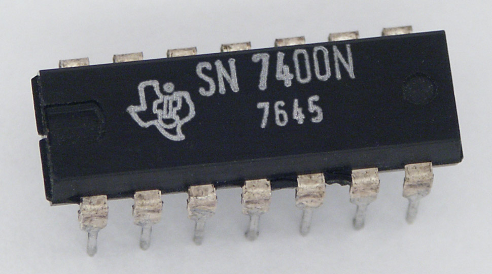
The 74xx series features a really broad range of gates and other things you can build with them. The 7400, for example, features four 2 input NAND gates on a single chip. This is the chip shown at the top of this post. Let’s look at the datasheet to figure out what those different pins do:
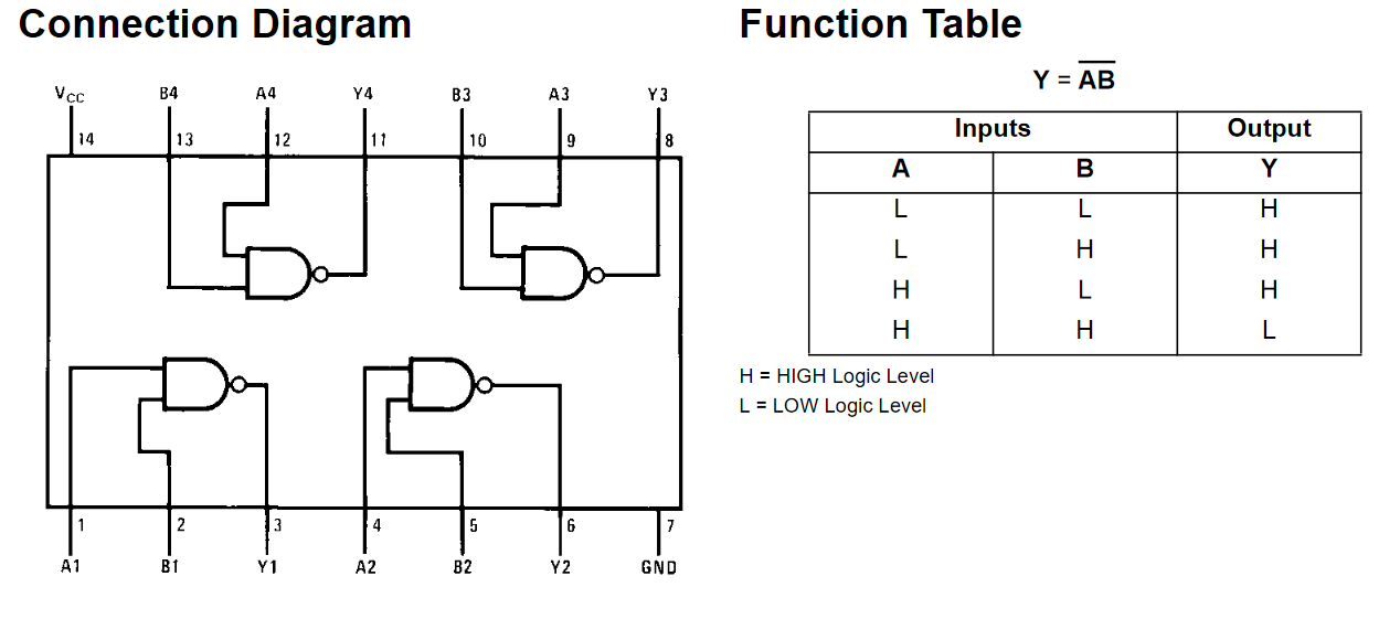
On the left, we see the connection diagram. Pin 14 (top left) and pin 7 (bottom right) supply power to the chip and are tied to 5V and ground, respectively. The other pins serve as inputs and output for the 4 gates, 12 in total. On the right, we can see the truth table. For any of the 4 gates, the output will be low (0V) when the inputs are both high (5V), and high otherwise.
This is convenient for us, as it means we won’t need to build anything out of discrete transistors. The series includes a lot of handy chips that we can make use of. You might notice in the examples featured above that we haven’t talked about how to actually store data, or latch a particular value for later use. All of our examples so far have outputs that are directly tied to whatever states the inputs are in. To store data, we can make constructs out of NAND gates called latches and flip-flops. We’ll discuss these in another post, but rather than constructing them with NAND gates, we’ll just use the 74xx series chips that already implement these constructs.
For the first cut of this project, however, I’m going to avoid chips like the 74ls181, which is a feature rich 4 bit ALU. If we wired two of these together, then we could have a complete 8 bit ALU with 32 total logic and arithmetic operations. This feels a little black-boxy, and considering that the ALU is an interesting component, I’d rather build something out of more easily understandable components, at least for the first implementation.
A great aspect of a project like this is how modular it is. As long as the individual components (ALU, registers, clock, control logic, etc) interface with the rest of the system in a (roughly) similar way, we can redesign each with minimal overall modification. This takes some pressure off of the first implementation, as we can always revisit modules as our goals and needs evolve.
Thanks for reading this far. In the next post I’ll talk about what the first implementation of the system might actually look like from an architecture perspective, and the modules that I’m planning on improving for subsequent iterations.
jc